



Proposed OSAT facility will target 2.5D/3D integration, chiplet architectures, hybrid bonding and co-packaged optics for AI and high-performance computing applications.
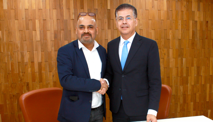
Paras Semiconductors, a subsidiary of Paras Defence & Space Technologies Limited, has entered into a strategic technology partnership with US-based BroadPak Corporation to develop advanced semiconductor packaging capabilities in India. The collaboration aims to establish an advanced heterogeneous integration and 3D packaging OSAT (Outsourced Semiconductor Assembly and Test) facility, strengthening India’s position in a critical segment of the semiconductor value chain.
The proposed facility will focus on 2.5D and 3D packaging, chiplet integration, hybrid bonding, wafer-level and panel-level fan-out packaging, co-packaged optics, and advanced semiconductor testing and qualification. These capabilities are increasingly important as demand for AI accelerators, high-performance computing (HPC), high-bandwidth memory and data-intensive applications pushes conventional chip architectures towards more sophisticated integration technologies.
Under the agreement, Paras Semiconductors will gain access to BroadPak’s intellectual property, design and manufacturing expertise, alongside technology transfer and process know-how in advanced packaging and chiplet integration. The companies will also explore joint development of packaging platforms for AI and HPC applications, as well as training programmes for Indian engineers.
BroadPak, headquartered in San Jose, California, has worked in 2.5D/3D IC packaging, heterogeneous integration, multi-die architectures, high-speed interconnects, thermal management and co-packaged optics since its establishment in 2007. Its capabilities span architecture, design, simulation, assembly, testing and production.
Munjal Sharad Shah, Managing Director of Paras Defence & Space Technologies, said the move represents a strategic expansion into a technology domain critical to India’s AI, data centre and industrial ambitions. The partnership will complement the company’s existing strengths in optics, optronics and critical electronics.
“Our collaboration with BroadPak brings the specialised technology expertise required to accelerate our ambition and develop capabilities that can serve both strategic domestic requirements and the wider semiconductor industry.”
— Munjal Sharad Shah, Managing Director, Paras Defence & Space Technologies Limited
Santosh Kumar, CEO of Paras Semiconductors, said the collaboration would help build capabilities in heterogeneous integration, chiplet architectures, hybrid bonding and system-in-package technologies to address the performance, connectivity and thermal requirements of next-generation semiconductor applications.
Dr. Farhang Yazdani, Founder and CEO of BroadPak Corporation, said India’s growing semiconductor ecosystem offers an opportunity to develop capabilities in advanced packaging and system-level integration. BroadPak will contribute its technology and manufacturing expertise to support the initiative.
The partnership comes amid growing global investment in advanced packaging. According to Yole Group estimates cited in the announcement, the global advanced packaging market is projected to expand from more than US$40 billion in 2024 to over US$80 billion by 2030.
For India, the initiative targets a crucial gap between wafer fabrication and the integration of semiconductor components into finished systems. By developing domestic capabilities in advanced packaging, Paras Semiconductors aims to serve strategic electronics requirements while addressing emerging demand from AI, networking and data centre markets.